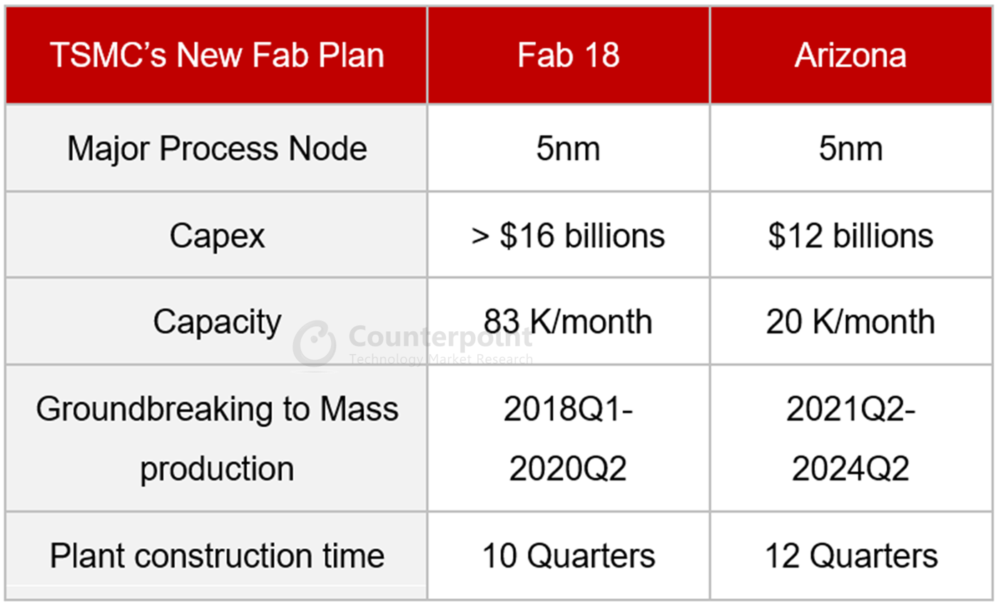
TSMC announced that it intends to build and operate an advanced semiconductor fab in Arizona, United States. This capacity of new fab will be 20K wafers per month with 5nm technology. Construction is planned to start in 2021 with mass production targeted to begin in 2024. The total investment in the project will be approximately US$12 billion from 2021 to 2029. This new facility will not only enable TSMC to better support its customers and partners, but it also gives TSMC more opportunities to attract global talent. The fab will enable leading U.S. companies to fabricate their cutting-edge semiconductor products within the United States.
Most of TSMC’s fabs are in Taiwan, and its global foundry share reached more than 50% in 2019, well ahead of its competitors. TSMC’s success is due to its large and diverse customer base and technical superiority over its competitors. Counterpoint Research believes that the construction of a new fab in the U.S. will help TSMC consolidate its leadership position. Compared to TSMC’s other 5nm fabs (Fab 18), its investment ($12 billion/20K) seems high while the period between breaking ground to initial mass production seems long. However, they could be prudent estimates considering this is TSMC’s first large-scale overseas plant.
Exhibit 1: The Comparison of TSMC Fab 18 and New Fab in Arizona
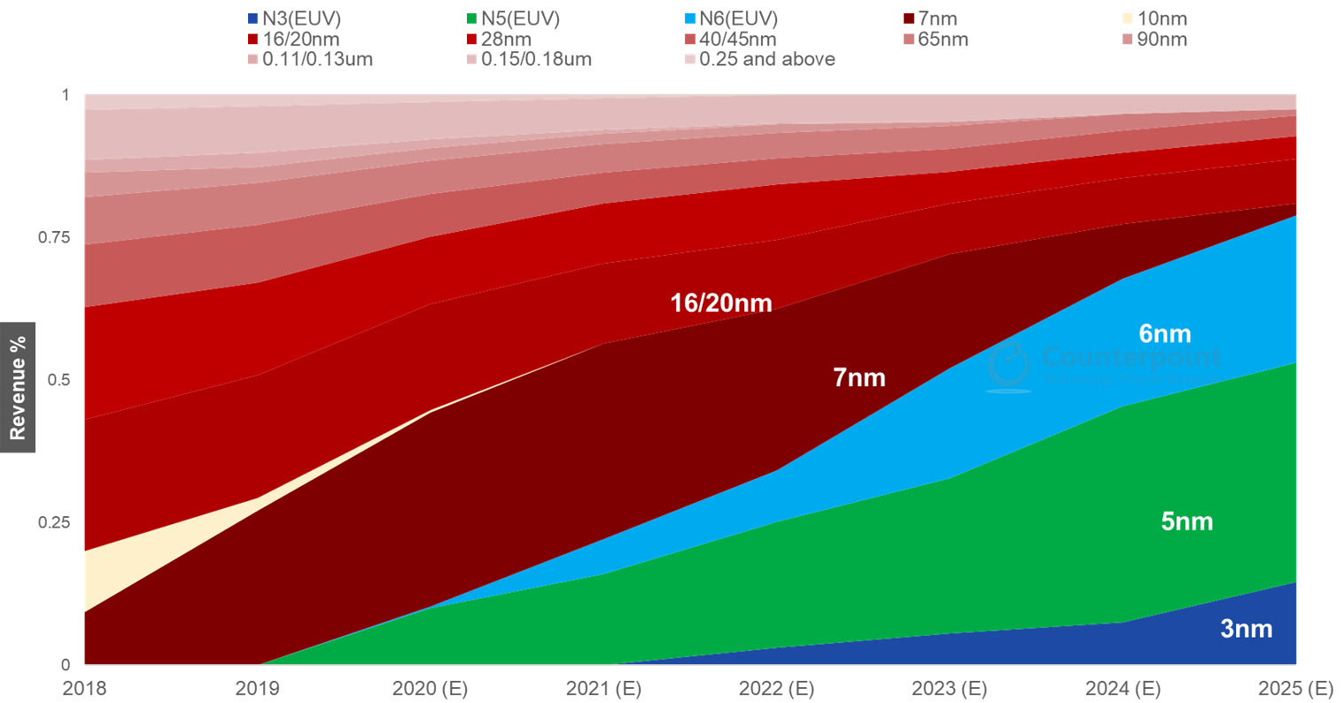
The share of 5nm in TSMC’s production is expected to reach 10% and 38.5% in 2020 and 2024, respectively. 3nm is expected to start mass production by 2022 and will take at least 2 to 3 years to ramp up. The chart below is Counterpoint Research’s forecast of TSMC’s process distribution over the next 5 years based on several assumptions and detailed analysis. Please contact Counterpoint to get more insights.
Exhibit 2: Forecast of TSMC Revenue by Technology, 2018-2025
The advantages of building new fab in U.S.
- As a company that plays a key role in the global electronics supply chain, TSMC has always had a need to diversify its manufacturing sites. TSMC has been Taiwan’s largest listed company by market value, and its main production base is also in Taiwan. As a result, the source of talent will gradually limit its growth. TSMC has a 12-inch wafer fab in Nanjing, China, with a 12/16nm process, however, TSMC has been unable to expand its China facility amid sensitive geopolitical issues. In addition, under the constraint of Wassenaar Arrangement, TSMC has difficulty in migrating its process node in its China fab to 7nm (EUV) and below.
- Another reason why TSMC needs to diversify its production base is the concern of the natural environment in Taiwan. Taiwan is in a seismically active zone, on the Pacific Ring of Fire. In the past, the “921 earthquakes” of 1999, with a magnitude as high as 7.3 on the Richter scale, caused a certain degree of damage to TSMC’s production. After than, TSMC has accumulated sufficient experience in preventing hazards caused by earthquakes. However, with TSMC now accounting for more than 50% market share and playing an even more critical role in the global electronics supply chain than in 1999, it is still prudent to diversify its production base.
- Over the next five years, the demand drivers for semiconductors will be automotive and consumer electronics. In order to achieve electrification, wireless connectivity, and autonomous driving, automotive electronics will require a large number and variants of semiconductors. The chips used in autonomous vehicles will require high-speed, but they don’t have to be as small as the chips in smartphones or laptops. On the other hand, reliability is very critical. Therefore, the manufacturing process node required for automotive electronics often doesn’t have to be the most advanced but has to be mature and reliable.
- The majority of TSMC’s manufacturing equipment is from American companies. According to our latest data, the share of the top three US semiconductor equipment companies (including AMAT, Lam Research, KLA) in total was more than 40% in 2019. Therefore, TSMC is able to get immediate support and is able to work efficiently with equipment suppliers to retrofit the equipment. In addition, the United States is also TSMC’s largest market. In 2019, the United States accounted for 45% of TSMC’s business. It can likely also get tax breaks and other incentives from Arizona.
The disadvantage of building new fab in U.S.
- The initial monthly capacity of TSMC’s Arizona plant is only 20,000 wafers. Therefore, other suppliers in the ecosystem are unlikely to follow TSMC to open a branch in the United States. However, if the operation of the new fab is running well and the demand is growing, it’s expected to see them follow TSMC to build a complete ecosystem there.
- Unlike memory manufacturing, the operation of foundry fab must be flexible in their production line to meet the different requirements for a variety of products while also maintain a high utilization rate. However, the new process development and initial mass production normally requires engineers to work overtime. In addition to the lower salaries than U.S. engineers, Taiwanese engineers have more flexible working hours and can complete time-consuming tasks such as new process optimization and troubleshooting. However, 5nm will be a relatively mature manufacturing process in 2024 and this new fab in the US is supposed to be highly automated, so there will likely be even less extra work for engineers in the new fab.
In summary, TSMC has more advantages than disadvantages in building its new fab in the U.S. by 2024. In addition to its superiority of technology over its competitors, TSMC’s success has been made by its large and diverse customer base. It has introduced different types of technology in each generation to meet the needs of various customers. 5nm is expected to account for about 38.5% of TSMC’s revenue in 2024 according to Counterpoint’s estimate. 5nm will be is a “long node” and a mature process, so the new fab will be highly automated in 2024. However, it can fulfill the demand for the largest number of applications. As a result, we believe TSMC’s 2024 fab in the U.S. can meet the needs of customers in the U.S. However, the state-of-art process will still be developed in Taiwan, where engineers will be relatively more flexible and the ecosystem will still be better.